ELE448: Digital Integrated Circuit Design I Cadence Tutorial
Create Circuit Schematic
Create New Library:
All designs related to a project/homework are stored in a library. To create a new library from the Library Manager, click on File > New > Library. In the New Library window, type lab-1 as the name of the library and click OK: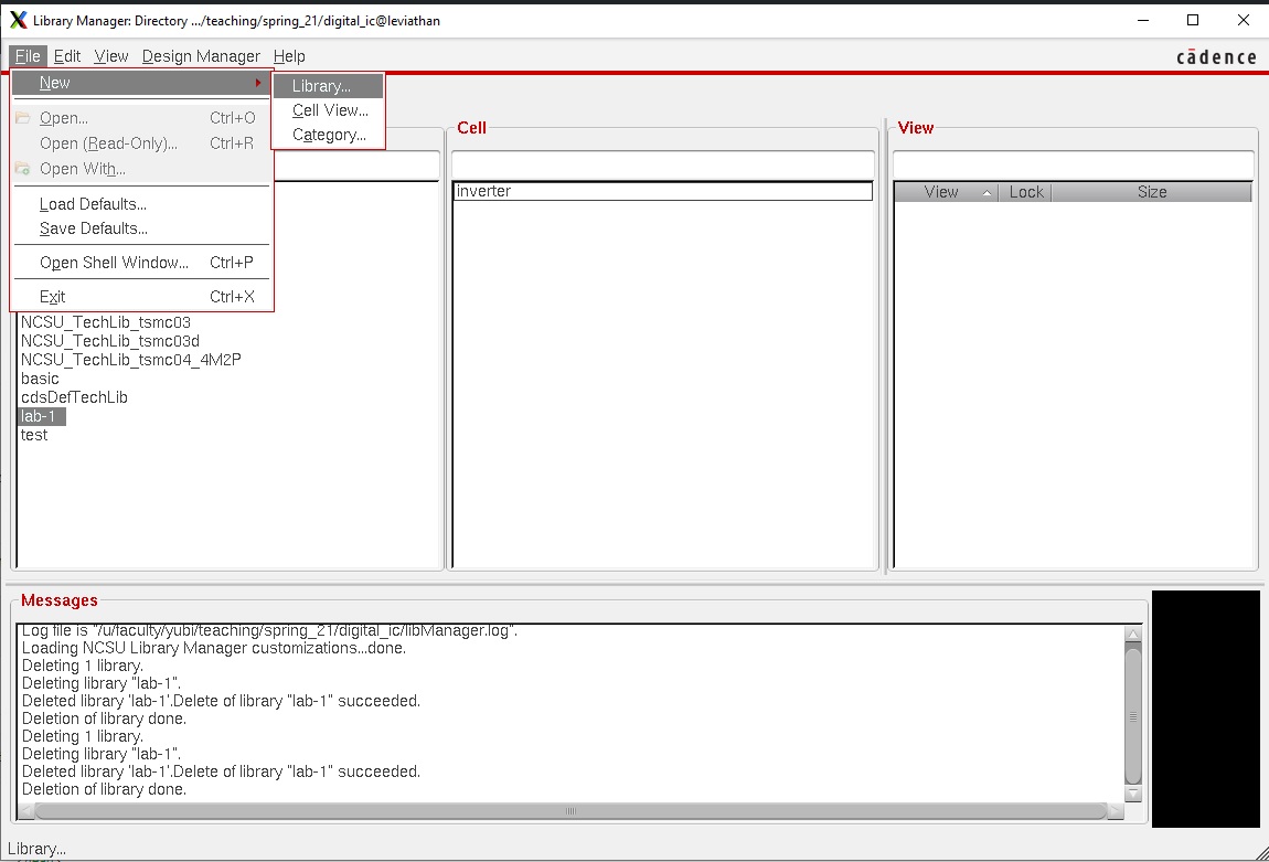
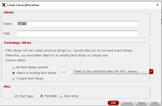
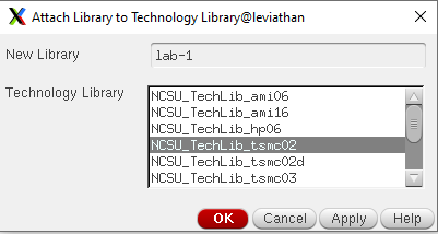
In the Technology Library, select attach to existing technology library, and choose TSMC 0.2u. Click OK
Now the library lab-1 is created.
Creating new schematic design:
In the Library Manager window, click on File > New > Cell View, and enter the following to create a schematic called Inverter and click OK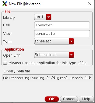
If the Upgrade License window appears, click Yes. The Virtuoso Schematic L tool appears, as shown below:
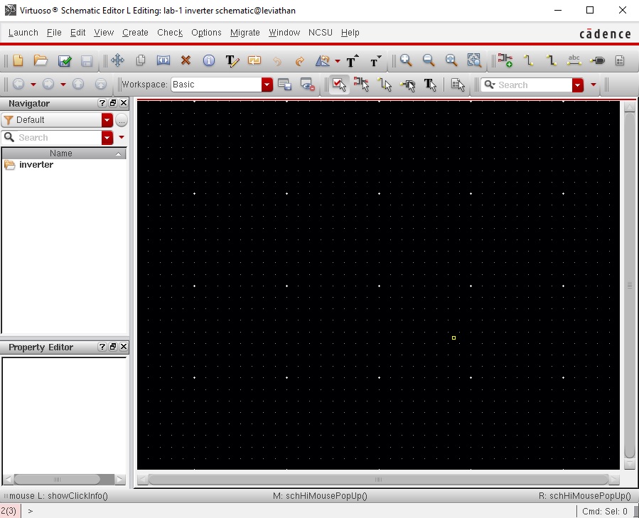
At this point, you have created a library called Lab1 and a cell inside it, called inverter. Now the design process can be started. For a full custom design, the process begins by creating a schematic. Then we simulate this design to verify the correctness of its functionality. Only after this is done, is the layout of the design performed.
Now, we put down the design of the inverter in the Schematic Editor window. The Inverter consists of a NMOS and PMOS transistor with appropriately connected gate, drain and source terminals. The transistors and the input signal sources are instantiated and connected in the schematic editor. To instantiate a NMOS transistor:
Create Instance:
In the schematic window, click on Create->Instance (or type i). The "Add instance" dialogue box appears together with the "component Browser" dialog box. (In case the "Component Browser" does not appear, click on browse in the "Add Instance" dialog box to start it.)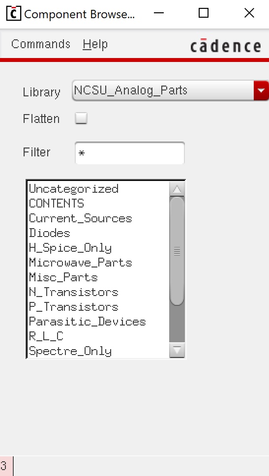
In "Component Browser" window, Click on Library and choose NCSU_Analog_Parts. Click on N_Transistors and choose nmos4 as your NMOS device. To place the instance, activate the schematic window and click the left mouse button to put the instance at the place desired.
Note in Cadence schematic composers and layout editors, a command will not terminate unless the user cancels it or the user starts a new command. In this case, you can see another instance is ready to be placed right after you placed the first instance. To terminate the current operation (which is "add instance" in this case), press ESC key on the keyboard. In fact, you can always cancel the current operation in schematic or layout editors by pressing ESC key.
Edit Object Properties:
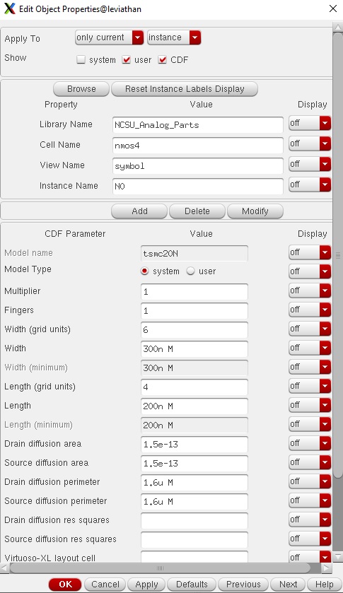
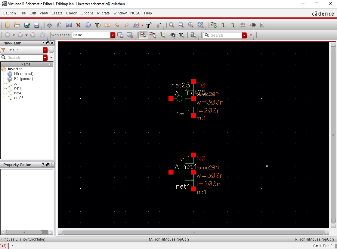
Now, we set the length and width of the NMOS transistor that is instantiated. To do this, select the object (NMOS transistor) by clicking on it and then go to "Edit > properties > Object..." (or by typing q). An object properties editing form will pop up. In this form, make the NMOS width 300n and length 200n, and click ok.
Repeat the Create Instance procedure for a PMOS transistor and set its width equal to 300n and length to 200n. The schematic should look similar to this:
Wiring up:
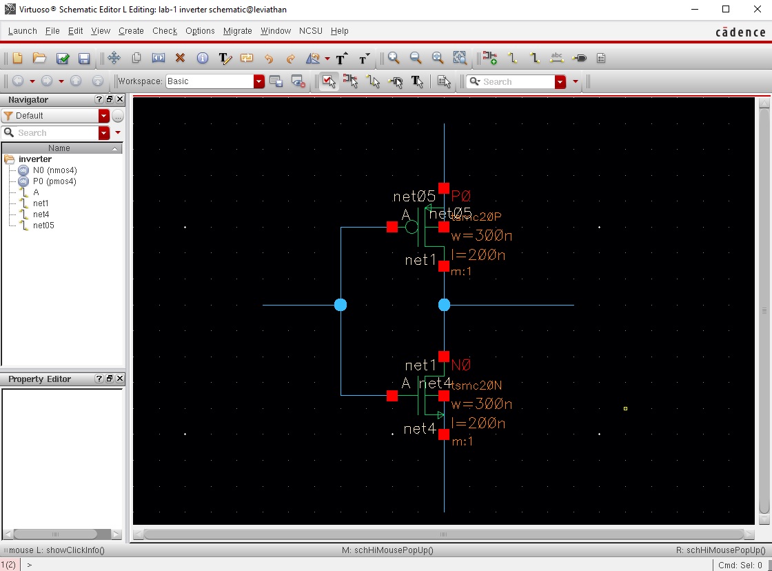
To connect the PMOS and NMOS devices or any electrical device, click on Create->Wire(narrow) in the schematic window (or type w). Click at the terminal where the wire starts and click at the terminal where the wire ends, a wire will be automatically added. If you are not satisfied with the automatic wiring, you can remove the wire and reroute it manually. This time, instead of clicking at the terminal where the wire ends directly, you can click the left mouse button whenever you want to change the wire direction.
If you want to stop the wire somewhere instead of connecting it to a terminal, double click your left mouse button and a dangling wire is created. In general dangling wire should be avoided, however, in some cases (like you want to label this wire or add a pin to this wire), a dangling wire makes sense.
In this case, connect the drain terminals of PMOS and NMOS, and the gate terminals of the PMOS and NMOS. Also, be sure to connect the bulk terminals of each transistor to its source. After all this wiring, the schematic should look similar to this :
Creating Supply Voltage Net (Vdd/gnd) and Input/Output pins:
Click on "Create->Pin..." (or type p) in the schematic window, the following dialogue box would appear:
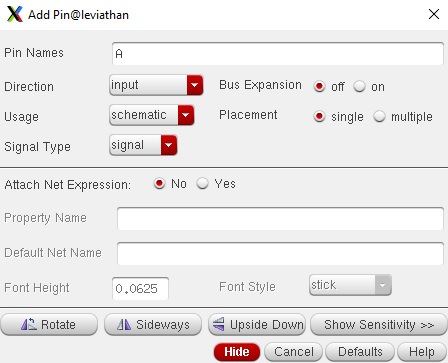
Type A as the pin name. Note that the direction is listed as input. For an output pin, you would need to change this to output. Now press Enter. Then in the schematic window, place the pin terminal on the wire that connects the gate terminals of the transistors. Similarly, create an Y pin and set its direction as output. The Y pin is placed on the wire connecting the drain terminals of the transistors. For VDD and GND, create VDD and GND pin and set its direction as inputOutput. After this, the schematic should look similar to this:
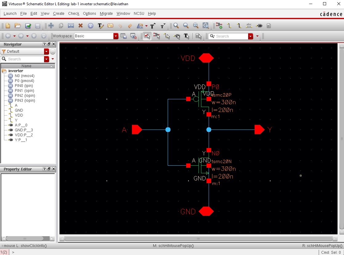
After the design has been completed, click on "File->Check and Save" to check and save your designs, or use hotkey F8. Check the CIW window to see if there are any errors or warnings in your design. If there are, then fix them and repeat Check & Save.
Create Circuit Symbol
Symbols are useful when the schematic design is done hierarchically. At a higher of level of abstraction, we would like to use a symbol to replace the details of a cell. Because of this, a symbol of a cell design should define all the input pins and output pins of that cell explicitly.Once you have completed the schematic design, you can create its symbol right from the schematic cell.
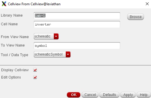
Click on Create > Cellview > From Cellview. Click OK on the Cellview From Cellview window and the next window.
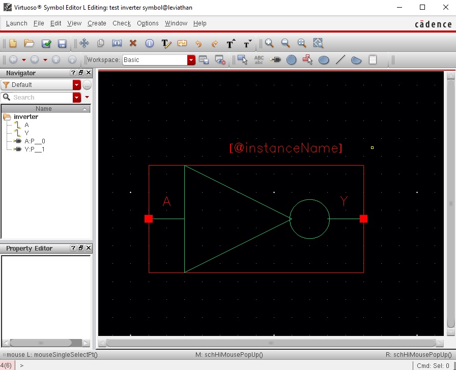
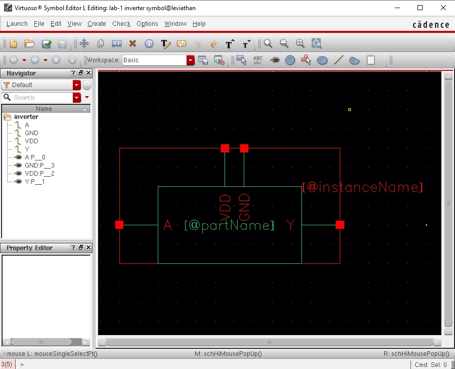
This will pop-up another window that contains a default symbol picture, which is shown below. It has a red box that encloses the green colored inverter symbol. This red box defines the actual size a symbol will occupy, if you were to use this inverter symbol in another design. You can change the size of this box by clicking and dragging. It is good custom to exactly fit the symbol within the red box. The red square dots indicate the pin connections. [@InstanceName ] and [@PartName] are display variables, which you may delete or keep. The following picture shows the symbol.
If you don't like this rectangular symbol that is automatically created by the tool, you can create a symbol of you own by dragging the lines and input/output pins to their desired locations. An example is shown below, in which an inverter symbol is created which looks similar to the usual inverter gate symbol: